Vigorous Input in Developing Semiconductor Materials Brings Opportunities for Laser Micro-processing in China
Huawei is again at the tip of public debate for both the ban imposed by U.S. Department of Commerce that is deemed as escalated chips prohibition and the Canadian court order against Meng Wanzhou, daughter of the founder of Huawei.
Sanction Imposed by U.S. Forced China to Pursue Indigenous Chips
The number of interest conflicts between China and America will only increase as a result of China’s rising national power and advancement of technological innovation. Sanctioned ZET in 2018 by the Trump administration was a clear warning to the Chinese people, followed by a series of opposition against Huawei and trade war in last year initiated by the American side. The unyielding position taken by the Chinese government has forced America back to the negotiation table. Out of the trade war have come a wave of self-reliance and self-inspiring in indigenous R&D and innovation for all sectors.
The most prominent sectors in American advanced technologies are semiconductors, chemical materials, software services, military industry, aerospace and bio-medicine. The route of global industrial development of semiconductor materials began in the well-known Silicon Valley of America and later stretched to Japan, Taiwan (China) and South Korea. The absence of attention to semiconductor materials and chips in China for a long period of time has resulted in the spending of trillions of RMB on imported chips annually. However, with a medium to long term development plan, China is committed to promoting the development of industry for indigenous integrated semiconductor circuit. And the conservative estimation of capital put in supporting R&D of chips industry reaches hundreds of billions in the years to come. Chips with high-tech content play a pivotal role in the industry. Mobile phones, computers, home appliances and navigation instruments all have chips embedded. But lithography machine, the core equipment for chip processing, is currently dominated by foreign countries.

The First Semiconductor Laser Cutter of Invisible Wafer in China
Into the Dawn of Laser Micro-processing Era, S&A Launched New Product
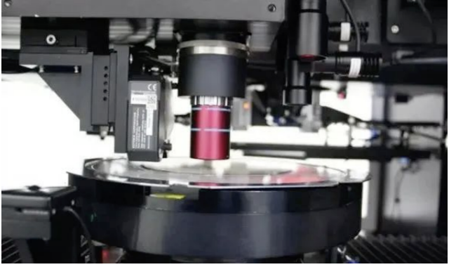
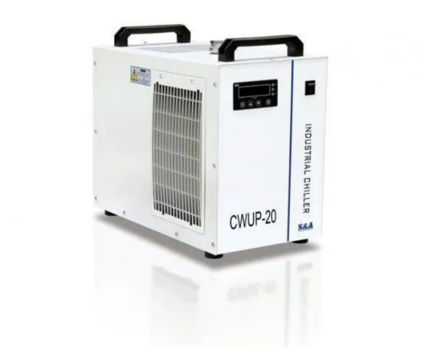
Entering the era of laser micro-processing, Guangzhou Teyu Electromechanical Co., Ltd. (also known as S&A) seizes the chance to launch water-chillers of ultra-precision. In retrospect of laser technological development of past years, laser has been well tapped in metal cutting and welding, but the application of ultra-precision laser manufacturing lags behind mainly because the former is rough processing and accuracy and customization for precise laser processing are very demanding. Its backwardness is further compounded by difficulties in developing new process and the long cycle. Precision work of laser chiefly evolves around consumer electronics with smart phones taking a large proportion. In the past several years, attention was also diverted to laser cutting of screens and OLED plates. In the future decade, semiconductor materials will become the most important industry in China. What might trigger an explosion of laser micro-processing is most likely the processing of semiconductor materials. Laser micro-processing requires laser machines of short pulse or ultra-short pulse, that is the ultra-fast laser. When national substantial input made in AI, 5G and semiconductor materials for indigenous development becomes a trend, laser micro-fabrication is set to be in huge demand and application of ultra-fast laser on a massive scale will be in vogue. Highly demanding ultra-fast laser of precision has prevented more companies from entering the market where only about 5 mature players have been established. Dozens of companies are now trying to access the market and develop products. Ultra-fast laser requests stable and controllable chillers of high precision and precise temperature control. In response to the development trend and market expectation of precision laser manufacturing in China, S&A first launched CWUP series of ultra-precision laser chiller, a breakthrough in temperature controlling technology for chillers by pushing the precision to ±0.1℃. It is suitable for diversified application scenarios such as ultra-fast solid-state laser chillers of picosecond and femtosecond, guaranteeing stability in precision laser process of semiconductor materials and electronic components. This product has been tested by a number of domestic and overseas light source brands, and is proved to be seamlessly compatible in terms of flow, pressure, electromagnetic flow, input and output, information exchange and docking, except for water temperature accuracy. In other words, this product could match any light source brands in the market. For the sake of saving cost on the user side, S&A empowered the product by expanding its power spectrum in application solutions to cover lasers of low, medium and high voltages.

Source: S&A

